PCB Layout Rules: Master the Art of PCB Design! Pcb design rules
Aight, listen up y'all, let's talk 'bout some PCB bidness. We talkin' 'bout them printed circuit boards, the real backbone of all our electronics. Without these thangs, ain't no phones, no TVs, no nothin'. So, lemme break it down for ya.
PCB layout design in PCB manufacturing

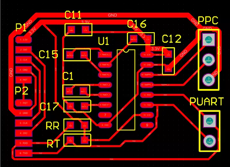
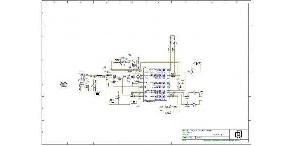
First off, we gotta talk 'bout the layout. This ain't just throwin' components on a board and hopin' for the best. Nah, this is science, art, and a whole lotta patience all rolled into one. The layout is how you arrange all them resistors, capacitors, chips, and other doohickeys on the board, and connect 'em all with them little copper traces. Think of it like city planning for electronics. You gotta think 'bout where everything goes, how it flows, and how to avoid traffic jams, aka, signal interference. A well-designed layout means a more efficient and reliable circuit.
Now, the engineers, they be spending hours, sometimes days, just figurin' this out. They use special software, CAD tools, to map everything out and make sure it all fits. It's like a giant puzzle, but instead of pieces, you got components, and instead of a picture, you got a circuit. They gotta consider things like heat dissipation, signal integrity, and manufacturing constraints. Can’t just dream up somethin' that can't even be made, ya know?
And don't even get me started on noise. That's unwanted electrical signals that can mess with your circuit. A good layout minimizes noise by keeping sensitive components away from noisy ones, and by using proper grounding techniques. Think of it like keepin' the peace in the neighborhood. You don't want no drama disturbin' the flow.
PCB layout rules

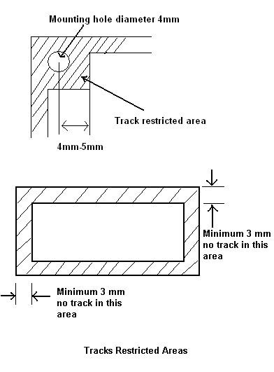
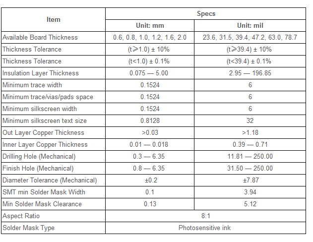
Now, onto them rules. Yeah, there's rules to this game, and you gotta follow 'em if you want your PCB to work right. We talkin' 'bout trace width, spacing, and all that technical mumbo jumbo. Trace width determines how much current a trace can carry. Too thin, and it'll overheat. Too thick, and you wastin' space. Spacing is how far apart the traces gotta be to avoid short circuits. Gotta keep 'em separated, like oil and water. And then there's via placement, ground planes, and a whole bunch of other things to keep in mind.
These rules ain't just arbitrary. They based on years of experience and scientific research. Engineers done learned the hard way what works and what don't. So, best to listen up and follow the guidelines. Think of it like the rules of the road. If you don't follow 'em, you gonna crash.
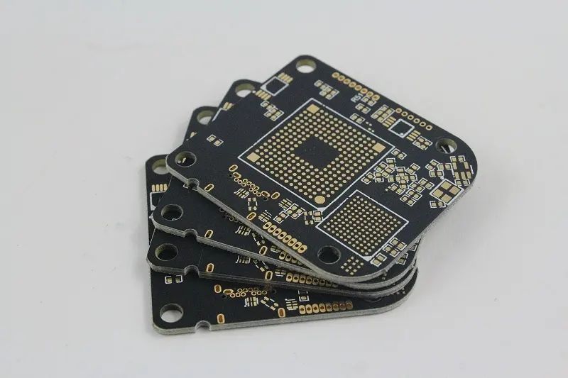
Bottom line, PCB layout is a critical part of the whole electronics manufacturing process. It takes skill, knowledge, and a whole lotta attention to detail. So, next time you usin' your phone or watchin' TV, take a moment to appreciate the complex engineering that went into makin' it all possible. It ain't magic, it's just good design.
If you are looking for PCB layout design in PCB manufacturing you've visit to the right place. We have 25 Pics about PCB layout design in PCB manufacturing like PCB Layout Rules and Limitations in PCB Design, Evatronix - PCB layout design and also Basic Steps to Design a PCB Layout – PCB HERO. Read more:
PCB Layout Design In PCB Manufacturing
pcbassemblymanufacturing.com PCB Design Layout Rules
 www.electronics-project-design.com
 Basic Rules Of PCB Design For High-Quality Circuit Boards
 hilelectronic.com
 Evatronix - PCB Layout Design
 evatronix.com
 pcb layout design hardware
PCB Layout Rules
www.linkedin.com Mastering Signal Tracing: Essential Rules For PCB Layout Design - 86PCB
 86pcb.com
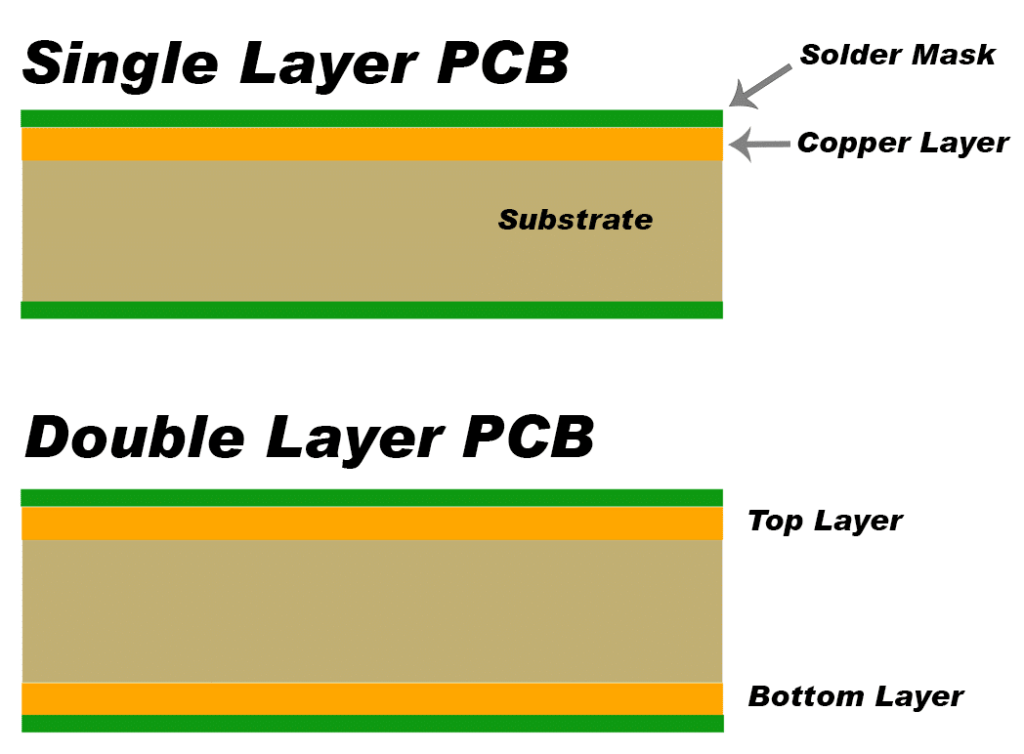
 How To Choose The Most Suitable Layer Number For PCB Design – PCB HERO
 www.pcb-hero.com
 PCB Design Rules For Electromagnetic Compatibility
 semiengineering.com
 PCB Layout Rules | Sierra Circuits
 www.protoexpress.com
 Pcb Design Rules - Specialistpowen
 specialistpowen.weebly.com
 PCB Layout Rules And Guidance - PCB & PCBA Manufacturer
 ipcb.co
 PCB Design Rules - Build Electronic Circuits
 www.build-electronic-circuits.com
 pcb rules seeed circuits build
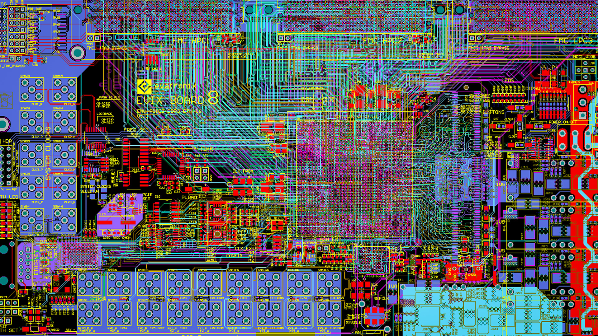
Evatronix - PCB Layout Design
 evatronix.com
 pcb design layout board printed circuits
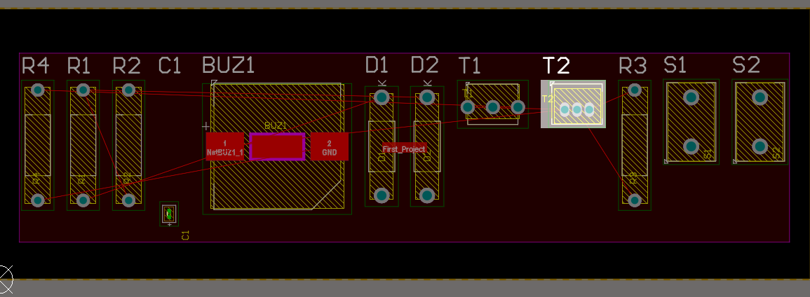
Basic Steps To Design A PCB Layout – PCB HERO
 www.pcb-hero.com
 PCB Factory Engineers Explain DDR PCB Layout Rules In Detail - Kingford
 www.kingfordpcb.com
 Ten Golden Rules Of PCB Design & Its Guidelines
 absolutepcbassembly.com
 Rigid-Flex PCB Layout Rules Free To PCB Design Engineers
 www.pcbae.com
 pcb flex rigid
PCB Design Layout Rules Recommendations - AiPCBA
 www.aipcba.com
 pcb recommendations adjacent
Pcb Express Design Rules
 pcbdesign.netlify.app
 Pcb Design Layout Guidelines Pcb Layout Guidelines For Design
 pcbways.pages.dev
 PCB Layout Rules And Limitations In PCB Design
 www.01pcb.com
 Pcb Train Design Rules - Heavy Wiring
 heavy-wiring.blogspot.com
 PCB Layout Rules - Exhibition - News
 www.oem-pcb.com
 A Detailed Guide To PCB Layout Design - IBE Electronics
 www.pcbaaa.com
 Mastering PCB Layout Design Rules For Optimal Circuit Performance - 86PCB
 86pcb.com
 Ten golden rules of pcb design & its guidelines. Basic rules of pcb design for high-quality circuit boards. Pcb layout rules